product properties:
| TYPE | DESCRIBE |
| category | Integrated Circuit (IC) Embedded - FPGA (Field Programmable Gate Array) |
| manufacturer | AMD Xilinx |
| series | Artix-7 |
| Package | tray |
| product status | in stock |
| Number of LAB/CLB | 4075 |
| Number of logic elements/units | 52160 |
| Total RAM bits | 2764800 |
| I/O count | 106 |
| Voltage - Powered | 0.95V ~ 1.05V |
| installation type | Surface Mount Type |
| Operating temperature | 0°C ~ 85°C (TJ) |
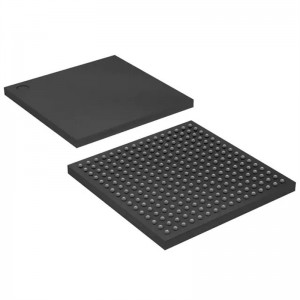
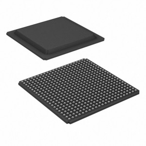
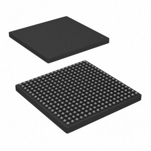
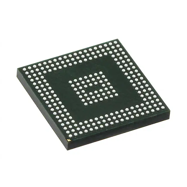
| Package/Enclosure | 238-LFBGA, CSPBGA |
| Supplier Device Packaging | 238-CSBGA (10x10) |
| Basic product number | XC7A50 |
report a bug
Environment and Export Classification:
| ATTRIBUTES | DESCRIBE |
| RoHS status | Compliant with ROHS3 specification |
| Moisture Sensitivity Level (MSL) | 3 (168 hours) |
| REACH status | Non-REACH products |
| ECCN | EAR99 |
| HTSUS | 8542.39.0001 |
DC Characteristics
Artix‐7 FPGAs Data Sheet:
DC and AC Switching Characteristics
DS181 (v1.27) February 10, 2022
Product Specification
Table 1: Absolute Maximum Ratings(1)
Symbol Description Min Max Units
FPGA Logic
VCCINT
Internal supply voltage –0.5 1.1 V
VCCAUX
Auxiliary supply voltage –0.5 2.0 V
VCCBRAM
Supply voltage for the block RAM memories –0.5 1.1 V
VCCO
Output drivers supply voltage for HR I/O banks –0.5 3.6 V
VREF
Input reference voltage –0.5 2.0 V
VIN(2)(3)(4)
I/O input voltage –0.4 VCCO + 0.55 V
I/O input voltage (when VCCO = 3.3V) for VREF and differential I/O standards
except TMDS_33(5)
–0.4 2.625 V
VCCBATT
Key memory battery backup supply –0.5 2.0 V
GTP Transceiver
VMGTAVCC
Analog supply voltage for the GTP transmitter and receiver circuits –0.5 1.1 V
VMGTAVTT
Analog supply voltage for the GTP transmitter and receiver termination circuits –0.5 1.32 V
VMGTREFCLK
Reference clock absolute input voltage –0.5 1.32 V
Table 2: Recommended Operating Conditions(1)(2)
Symbol Description Min Typ Max Units
FPGA Logic
VCCINT(3)
For -3, -2, -2LE (1.0V), -1, -1Q, -1M devices: internal supply voltage 0.95 1.00 1.05 V
For -1LI (0.95V) devices: internal supply voltage 0.92 0.95 0.98 V
For -2LE (0.9V) devices: internal supply voltage 0.87 0.90 0.93 V
VCCAUX
Auxiliary supply voltage 1.71 1.80 1.89 V
VCCBRAM(3)
For -3, -2, -2LE (1.0V), -2LE (0.9V), -1, -1Q, -1M devices: block RAM supply
voltage
0.95 1.00 1.05 V
For -1LI (0.95V) devices: block RAM supply voltage 0.92 0.95 0.98 V
VCCO(4)(5)
Supply voltage for HR I/O banks 1.14 – 3.465 V
VIN(6)
I/O input voltage –0.20 – VCCO + 0.20 V
I/O input voltage (when VCCO = 3.3V) for VREF and differential I/O standards
except TMDS_33(7)
–0.20 – 2.625 V
IIN(8)
Maximum current through any pin in a powered or unpowered bank when
forward biasing the clamp diode.
– – 10 mA
VCCBATT(9)
Battery voltage 1.0 – 1.89 V
GTP Transceiver
VMGTAVCC(10)
Analog supply voltage for the GTP transmitter and receiver circuits 0.97 1.0 1.03 V
VMGTAVTT(10)
Analog supply voltage for the GTP transmitter and receiver termination circuits 1.17 1.2 1.23 V