product properties:
| TYPE | DESCRIBE |
| category | Integrated Circuit (IC) Embedded - FPGA (Field Programmable Gate Array) |
| manufacturer | AMD Xilinx |
| series | Spartan®-6 LX |
| Package | tray |
| product status | in stock |
| Number of LAB/CLB | 300 |
| Number of logic elements/units | 3840 |
| Total RAM bits | 221184 |
| I/O count | 106 |
| Voltage - Powered | 1.14V ~ 1.26V |
| installation type | Surface Mount Type |
| Operating temperature | 0°C ~ 85°C (TJ) |
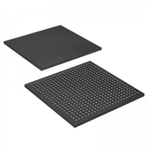
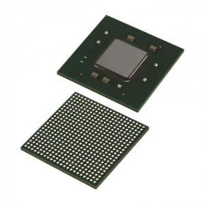
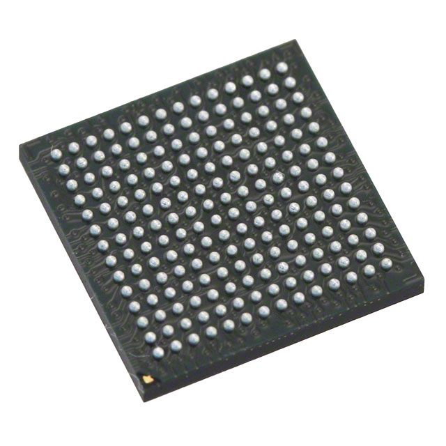
| Package/Enclosure | 196-TFBGA, CSBGA |
| Supplier Device Packaging | 196-CSPBGA (8x8) |
| Basic product number | XC6SLX4 |
report a bug
Environment and Export Classification:
| ATTRIBUTES | DESCRIBE |
| RoHS status | Compliant with ROHS3 specification |
| Moisture Sensitivity Level (MSL) | 3 (168 hours) |
| REACH status | Non-REACH products |
| ECCN | EAR99 |
| HTSUS | 8542.39.0001 |
Notes:
1. Stresses beyond those listed under Absolute Maximum Ratings might cause permanent damage to the device. These are stress ratings
only, and functional operation of the device at these or any other conditions beyond those listed under Operating Conditions is not implied.
Exposure to Absolute Maximum Ratings conditions for extended periods of time might affect device reliability.
2. When programming eFUSE, VFS ≤ VCCAUX. Requires up to 40 mA current. For read mode, VFS can be between GND and 3.45 V.
3. I/O absolute maximum limit applied to DC and AC signals. Overshoot duration is the percentage of a data period that the I/O is stressed
beyond 3.45V.
4. For I/O operation, refer to UG381: Spartan-6 FPGA SelectIO Resources User Guide.
5. Maximum percent overshoot duration to meet 4.40V maximum.
6. TSOL is the maximum soldering temperature for component bodies. For soldering guidelines and thermal considerations,
see UG385: Spartan-6 FPGA Packaging and Pinout Specification.
Recommended Operating Conditions(1)
Symbol Description Min Typ Max Units
VCCINT
Internal supply voltage relative to GND
-3, -3N, -2 Standard performance(2)
1.14 1.2 1.26 V
-3, -2 Extended performance(2)
1.2 1.23 1.26 V
-1L Standard performance(2)
0.95 1.0 1.05 V
VCCAUX(3)(4) Auxiliary supply voltage relative to GND
VCCAUX = 2.5V(5)
2.375 2.5 2.625 V
VCCAUX = 3.3V 3.15 3.3 3.45 V
VCCO(6)(7)(8) Output supply voltage relative to GND 1.1 – 3.45 V
VIN
Input voltage relative to GND
All I/O
standards
(except PCI)
Commercial temperature (C) –0.5 – 4.0 V
Industrial temperature (I) –0.5 – 3.95 V
Expanded (Q) temperature –0.5 – 3.95 V
PCI I/O standard(9)
–0.5 – VCCO + 0.5 V
IIN(10)
Maximum current through pin using PCI I/O standard
when forward biasing the clamp diode.(9)
Commercial (C) and
Industrial temperature (I)
– – 10 mA
Expanded (Q) temperature – – 7 mA
Maximum current through pin when forward biasing the ground clamp diode. – – 10 mA
VBATT(11)
Battery voltage relative to GND, Tj = 0°C to +85°C
(LX75, LX75T, LX100, LX100T, LX150, and LX150T only)
1.0 – 3.6 V
Tj
Junction temperature operating range
Commercial (C) range 0 – 85 °C
Industrial temperature (I) range –40 – 100 °C
Expanded (Q) temperature range –40 – 125 °C
Notes:
1. All voltages are relative to ground.
2. See Interface Performances for Memory Interfaces in Table 25. The extended performance range is specified for designs not using the
standard VCCINT voltage range. The standard VCCINT voltage range is used for:
• Designs that do not use an MCB
• LX4 devices
• Devices in the TQG144 or CPG196 packages
• Devices with the -3N speed grade
3. Recommended maximum voltage droop for VCCAUX is 10 mV/ms.
4. During configuration, if VCCO_2 is 1.8V, then VCCAUX must be 2.5V.
5. The -1L devices require VCCAUX = 2.5V when using the LVDS_25, LVDS_33, BLVDS_25, LVPECL_25, RSDS_25, RSDS_33, PPDS_25,
and PPDS_33 I/O standards on inputs. LVPECL_33 is not supported in the -1L devices.
6. Configuration data is retained even if VCCO drops to 0V.
7. Includes VCCO of 1.2V, 1.5V, 1.8V, 2.5V, and 3.3V.
8. For PCI systems, the transmitter and receiver should have common supplies for VCCO.
9. Devices with a -1L speed grade do not support Xilinx PCI IP.
10. Do not exceed a total of 100 mA per bank.
11. VBATT is required to maintain the battery backed RAM (BBR) AES key when VCCAUX is not applied. Once VCCAUX is applied, VBATT can be
unconnected. When BBR is not used, Xilinx recommends connecting to VCCAUX or GND. However, VBATT can be unconnected.