product properties:
| TYPE | DESCRIBE |
| category | Integrated Circuit (IC) Embedded - FPGA (Field Programmable Gate Array) |
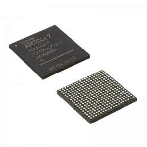
| manufacturer | AMD Xilinx |
| series | Spartan®-6 LX |
| Package | tray |
| product status | in stock |
| Number of LAB/CLB | 1139 |
| Number of logic elements/units | 14579 |
| Total RAM bits | 589824 |
| I/O count | 232 |
| Voltage - Powered | 1.14V ~ 1.26V |
| installation type | Surface Mount Type |
| Operating temperature | -40°C ~ 100°C (TJ) |
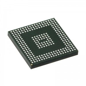
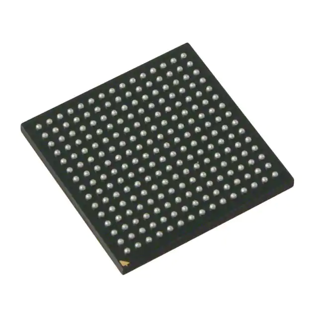
| Package/Enclosure | 324-LFBGA, CSPBGA |
| Supplier Device Packaging | 324-CSPBGA (15x15) |
| Basic product number | XC6SLX16 |
report a bug
New Parametric Search
Environment and Export Classification:
| ATTRIBUTES | DESCRIBE |
| RoHS status | Compliant with ROHS3 specification |
| Moisture Sensitivity Level (MSL) | 3 (168 hours) |
| REACH status | Non-REACH products |
| ECCN | 3A991D |
| HTSUS | 8542.39.0001 |
Notes:
1. All voltages are relative to ground.
2. See Interface Performances for Memory Interfaces in Table 25. The extended performance range is specified for designs not using the
standard VCCINT voltage range. The standard VCCINT voltage range is used for:
• Designs that do not use an MCB
• LX4 devices
• Devices in the TQG144 or CPG196 packages
• Devices with the -3N speed grade
3. Recommended maximum voltage droop for VCCAUX is 10 mV/ms.
4. During configuration, if VCCO_2 is 1.8V, then VCCAUX must be 2.5V.
5. The -1L devices require VCCAUX = 2.5V when using the LVDS_25, LVDS_33, BLVDS_25, LVPECL_25, RSDS_25, RSDS_33, PPDS_25,
and PPDS_33 I/O standards on inputs. LVPECL_33 is not supported in the -1L devices.
6. Configuration data is retained even if VCCO drops to 0V.
7. Includes VCCO of 1.2V, 1.5V, 1.8V, 2.5V, and 3.3V.
8. For PCI systems, the transmitter and receiver should have common supplies for VCCO.
9. Devices with a -1L speed grade do not support Xilinx PCI IP.
10. Do not exceed a total of 100 mA per bank.
11. VBATT is required to maintain the battery backed RAM (BBR) AES key when VCCAUX is not applied. Once VCCAUX is applied, VBATT can be
unconnected. When BBR is not used, Xilinx recommends connecting to VCCAUX or GND. However, VBATT can be unconnected.Spartan-6 FPGA Data Sheet: DC and Switching Characteristics
DS162 (v3.1.1) January 30, 2015
www.xilinx.com
Product Specification
4
Table 3: eFUSE Programming Conditions(1)
Symbol Description Min Typ Max Units
VFS(2)
External voltage supply
3.2 3.3 3.4 V
IFS
VFS supply current
– – 40 mA
VCCAUX Auxiliary supply voltage relative to GND 3.2 3.3 3.45 V
RFUSE(3) External resistor from RFUSE pin to GND 1129 1140 1151
Ω
VCCINT
Internal supply voltage relative to GND 1.14 1.2 1.26 V
tj
Temperature range
15 – 85 °C
Notes:
1. These specifications apply during programming of the eFUSE AES key. Programming is only supported through JTAG.The AES key is only
supported in the following devices: LX75, LX75T, LX100, LX100T, LX150, and LX150T.
2. When programming eFUSE, VFS must be less than or equal to VCCAUX. When not programming or when eFUSE is not used, Xilinx
recommends connecting VFS to GND. However, VFS can be between GND and 3.45 V.
3. An RFUSE resistor is required when programming the eFUSE AES key. When not programming or when eFUSE is not used, Xilinx
recommends connecting the RFUSE pin to VCCAUX or GND. However, RFUSE can be unconnected.